User:Nzebro12/sandbox
The Pixel Visual Core (PVC) is a series of ARM-based System in Package (SiP) image processors designed by Google.[1] The PVC is a fully programmable Image, Vision and AI multi-core domain-specific architecture(DSA) for mobile devices and in future for IoT.[2]
It first appeared in the Google Pixel 2 and 2 XL which were introduced on October 19, 2017. It has also appeared in the Google Pixel 3 and 3 XL.
History
[edit]Google previously used Qualcomm Snapdragon's CPU, GPU, IPU, and DSP to handle its image processing for their Google Nexus and Google Pixel devices. With the increasing importance of computational photography techniques, Google developed the Pixel Visual Core (PVC). Google claims the PVC uses less power than using CPU and GPU while still being fully programmable, unlike their Tensor processing unit (TPU) application-specific integrated circuit (ASIC). Indeed, classical mobile devices equip an image signal processor (ISP) that is a fixed functionality image processing pipeline. In contrast to this, the PVC has a flexible programmable functionality, not limited only to image processing.
The PVC in the Google Pixel 2 and 2 XL is labeled SR3HX X726C502.[3]
The PVC in the Google Pixel 3 and 3 XL is labeled SR3HX X739F030.[4]
Thanks to the PVC, the Pixel 2 and Pixel 3 obtained a mobile DxOMark of 98[5] and 101.[6] The latter one is the top-ranked single-lens mobile DxOMark score, tied with the iPhone XR.[7]
Pixel Visual Core software
[edit]
A typical image-processing program of the PVC is written in Halide. Currently, it supports just a subset of Halide programming language without floating point operations and with limited memory access patterns.[8] Halide is a widely adopted domain specific language that lets the user decouple the algorithm and the scheduling of its execution. In this way, the developer can write a program that is optimized for the target hardware architecture.[9]
Pixel Visual Core ISA
[edit]The PVC has two types of Instruction Set Architecture (ISA) a virtual and a physical one. First, a high-level language program is compiled into a virtual ISA (vISA), inspired by RISC-V ISA [9], that abstracts completely from the target hardware generation. Then, the vISA program is compiled into the so called physical ISA (pISA), that is a VLIW ISA. This compilation step takes into account the target hardware parameters, like array of PEs size, STP size, etc. and specify explicitly memory movements. The decoupling of vISA and pISA lets the first one to be cross-architecture and generation-independent, while pISA can be compiled offline or through JIT compilation [8]
Pixel Visual Core architecture
[edit]
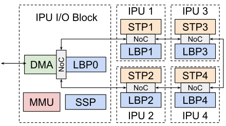
The Pixel Visual Core is designed to be a scalable multi-core energy-efficient architecture. The core of a PVC is the Image Processing Unit (IPU) a programmable unit tailored for image processing.
Image Processing Unit (IPU)
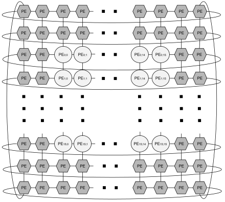
[edit]The IPU core has a Stencil Processor (STP), a Line Buffer Pool (LBP) and a NoC. The STP mainly provides a 2-D SIMD array of Processing Elements (PEs) able to perform stencil computations, a small neighborhood of pixels. Though it seems similar to systolic array and wavefront computations, the STP has an explicit software controlled data movement.[9]
Line Buffer Pool (LBP)
[edit]Considering that one of the most energy costly operation is DRAM access, each STP has temporary buffers to increase data locality, namely LBP. The used LBP is a 2-D FIFO that accommodates different sizes of reading and writing. The LBP uses single-producer multi-consumer behavioral model. Each LBP can have eight logical LB memories and one for DMA input-output operations.[8] Due to the real high complexity of the memory system, the PVC designers state the LBP controller as one of the most challenging components.[9] The NoC used is a ring network on chip used to communicate with only neighbor cores for energy savings and pipelined computational pattern preservation.[9]
Stencil Processor (STP)
[edit]
The STP has a 2-D array of PEs, for example, a 16x16 array of full PEs and four lanes of simplified PEs called "halo". The STP has a scalar processor, called scalar lane (SCL), that adds control instructions with a small instruction memory. The last component of an STP is a load store unit called Sheet Generator (SHG), where the sheet is the PVC memory access unit.[9]
SR3HX design summary
[edit]The SR3HX PVC features a 64-bit ARMv8a ARM Cortex-A53 CPU, 8x Image Processing Unit (IPU) cores, 512 MB LPDDR4, MIPI, PCIe. The IPU cores each have 512 Arithmetic Logic Units (ALUs) consisting of 256 processing elements (PEs) arranged as a 16 x 16 2-dimensional array. Those cores execute a custom VLIW ISA. There are two 16-bit ALUs per processing element and they can operate in three distinct ways: independent, joined, and fused.[10] The SR3HX PVC is manufactured as a SiP by TSMC using their 28HPM HKMG process.[1] It was designed over 4 years in partnership with Intel. (Codename: Monette Hill)[11] Google claims the SR3HX PVC is 7-16x more energy-efficient than the Snapdragon 835.[1] And that the SR3HX PVC can perform 3 trillion operations per second, HDR+ can run 5x faster and at less than one-tenth the energy than the Snapdragon 835.[12] It supports Halide for image processing and TensorFlow for machine learning.[12]. The current chip runs at 426MHz[9] and the single IPU is able to perform more than 1 TeraOPS.[8]
See also
[edit]- Google Pixel devices, range of consumer hardware designed by Google
- Tensor processing unit (TPU), Google design ASICs for neural network machine learning processing.
References
[edit]- ^ a b c Cutress, Ian. "Hot Chips 2018: The Google Pixel Visual Core Live Blog (10am PT, 5pm UTC)". www.anandtech.com. Retrieved 2019-02-02.
- ^ Hennessy, John; Patterson, David. Computer architecture : a quantitative approach (Sixthition ed.). Morgan Kaufmann. ISBN 978-0128119051.
- ^ "Google Pixel 2 XL Teardown". iFixit. 2017-10-19. Retrieved 2019-02-02.
- ^ "Google Pixel 3 XL Teardown". iFixit. 2018-10-16. Retrieved 2019-02-02.
- ^ "Pixel 2 DxOMark".
- ^ "Pixel 3 DxOMark".
- ^ "iPhone XR DxOMark".
- ^ a b c d "The Pixel Visual Core: Google's Fully Programmable Image, Vision and AI Processor for Mobile Devices. HotChips2018" (PDF).
- ^ a b c d e f g Hennessy, John; Patterson, Davide (2017). Computer architecture : a quantitative approach (Sixth edition ed.). Morgan Kaufmann. pp. 579–592. ISBN 978-0128119051.
{{cite book}}:|edition=has extra text (help) - ^ "Pixel Visual Core (PVC) - Google - WikiChip". en.wikichip.org. Retrieved 2019-02-02.
- ^ "Google Partnered with Intel for the Pixel Visual Core Chip in the Pixel 2". xda-developers. 2017-10-25. Retrieved 2019-02-02.
- ^ a b "Pixel Visual Core: image processing and machine learning on Pixel 2". Google. 2017-10-17. Retrieved 2019-02-02.

